A Study on the Modeling of Flyback Converter for LED Power Based on State-space Averaging
Abstract
Switch mode power supply is a high-frequency electrical energy conversion apparatus that is widely used in many home appliances, industrial products, and military applications. In this study, a Flyback converter with LED as the load is modeled. To verify the system stability, a pulse-width modulated switching control circuit is evolved into a small-signal model with linear characteristics based on state-space averaging. Through MATLAB simulation results, it is shown that the current-control mode is superior to the voltage-control mode. A DC 46 V LED power output closed-loop feedback control switching power supply is fabricated, and the experimental and simulation results verify the superiority of the design. From this study, the current control mode is suitable for the use in flyback LED switching power supplies because the current mode method shows more stable characteristics with GM = 11.975 dB and PM = 46.073°.
Keywords:
Flyback Converter, State-space Averaging, Modeling, LED Power, Voltage Control1. Introduction
Compared to conventional lighting, lamps made of light-emitting diodes (LEDs) are energy efficient, environmentally friendly, long-lasting, and have good color rendering and responsiveness.1) The flyback converter used as a constant-voltage power supply for LED loads in this study is an isolated converter topology.1-4)
Flyback converters are widely used in low-power applications owing to their simple structure, low cost, high efficiency, low component count, and possibility of buck/boost operation.5-14) The continuous-time model of the flyback converter was proposed by Ridley15) and Middlebrook,16) this model is suitable for studying the small-signal dynamics of the current-mode control of the converter through frequency analysis.15,16)
Choi17) analyzed the step response of the load through the transfer function, and Erickson18) analyzed the characteristics of the converter via large-signal modeling. In the analysis of various converter models, it is common practice to analyze the converter characteristics with a Bode plot on the frequency plane based on loop-gain analysis using the state-space averaging method.19,20) To simplify the design, flyback switching converters are generally modeled using state-space averaging techniques in the ideal state to obtain a linear system model.21-26)
In this study, based on the change characteristics of the LED internal resistance according to voltage, the voltage-control and current-control methods of the flyback converter were analyzed via MATLAB simulation. The proposed current mode control T2(s) with GM = 11.975 dB, PM = 46.073° is obtained and its phase change is seen to be gradually slow, and it can be determined that the system will operate stably in LED lighting.
Based on the simulation results, the characteristics were compared and analyzed using the Bode and root-locus plots. A prototype flyback converter was constructed for 20W LED power, and its feasibility was confirmed through PSIM simulation and experiments. It can also be verified by the experimental results that the current control mode has a stable pulse-width modulation effect on the duty cycle of the switching signal.
2. Flyback Conversion System and Control Mode
Fig. 1 shows the LED power supply system, including the power conversion, system control, and comparison feedback circuits.
An electromagnetic interference (EMI) filter is used to remove the EMI from the high-frequency pulses in the power supply, and the input AC voltage is converted to DC-DC power supply after full-bridge rectification.1-4)
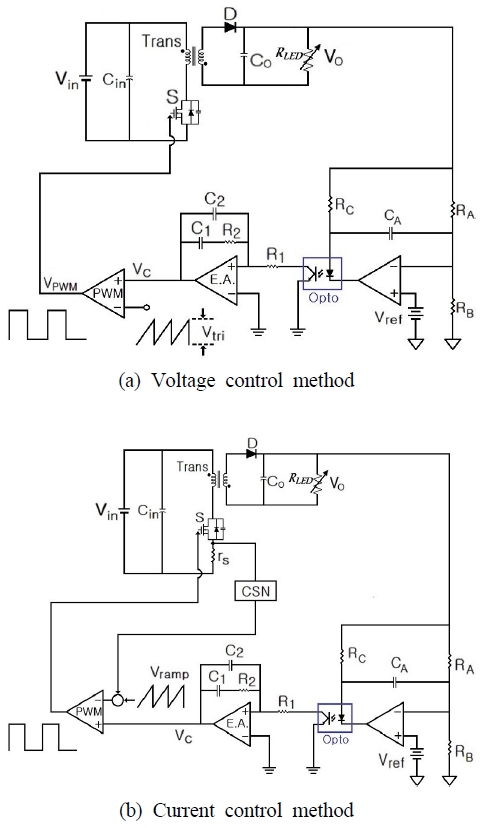
Fig. 2 shows the voltage and current feedback control methods for the flyback converter.20) Fig. 2(a) is the voltage control method, where the feedback voltage is compared with the reference voltage(Vref) and the feedback control voltage(Vc) is output through the optocoupler(Opto) and voltage controller. Fig. 2(b) is the current controlmethod, where the detected current through the resistor(rs) of the switch(S) plus a carrier wave(Vramp) is fed to the controller as a feedback signal simultaneously with the feedback control voltage(Vc).20)
3. Modeling of Flyback Converter
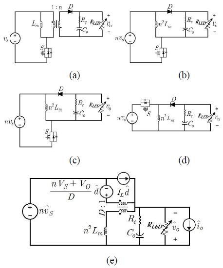
The equivalent models of the flyback converter are shown in Fig. 3.20)
Fig. 3(a) is the original flyback converter, and Fig. 3(b) and Fig. 3(c) are the modified models.
The flyback converter becomes a buck-boost epuivalent circuit, as shown in Fig. 3(d), where the transformer winding turns ratio is 1 : n, input voltage of the equivalent converter is nVs, and equivalent inductor is n2Lm. Fig. 3(e) is small-signal model of the converter. The transfer function of the duty cycle output voltage in the flyback converter is shown in equation (1).20)
| (1) |
where
- (a) Original flyback converter
- (b) Modified model(1)
- (c) Modified model(2)
- (d) Equivalent buck/boost converter
- (e) Small-signal model
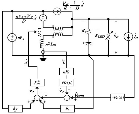
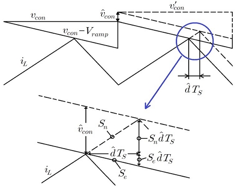
Fig. 4 shows the small-signal model of the flyback converter for the current control mode, and Fig. 5 shows the modulator waveform with a microwave perturbed control voltage.20)
From Fig. 5, the relationship between and the following equations (2) and (3) can be seen.20)
| (2) |
| (3) |
From equation (2), the F* of the current control mode can be expressed as in equation (4).20)
| (4) |
where:
According to Mason's rule, the transfer function Hi(s) of the control voltage and inductor current of the flyback converter in the current control mode is obtained form equations (5) and (6) below.20)
| (5) |
| (6) |
where,
Next, according to Mason's rule, the transfer function Gvci(s) of the system control voltage and output voltage can be expressed using equations (7) and (8).20)
| (7) |
| (8) |
where,
4. Design of Voltage Feedback Controller for Flyback Converter with Loop Gain
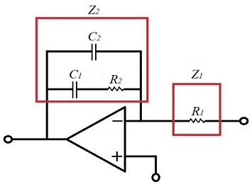
Fig. 6 shows a two-pole single-zero voltage compensator used as the voltage feedback controller for the flyback converter in this study, and its transfer function Fv(s) is as shown in equation (9).20)
| (9) |
where,
Therefore, according to Mason's rule, the loop transfer function T1(s) for the voltage control mode of the flyback converter is as shown in equation (10), and the loop transfer function T2(s) for the current control mode is as shown in equation (11).20)
| (10) |
| (11) |
5. MATLAB Simulation: Comparison of Voltage-mode and Current-mode Control Characteristics
Table 1 shows the simulated circuit components and system parameters of the flyback converter obtained using MATLAB.
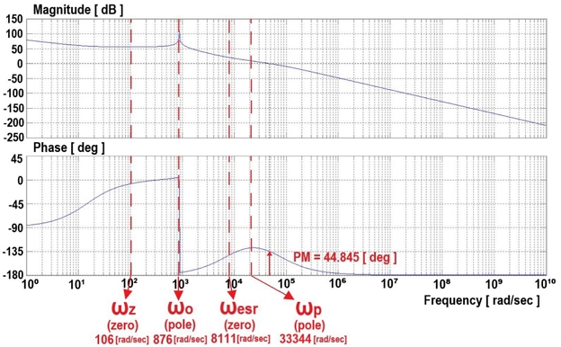
Fig. 7 is the Bode plot of the duty-ratio-to–output-voltage Gvd(s) and Fig. 8 is the Bode plot of T1(s) in the voltage control mode.
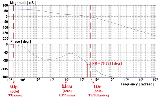
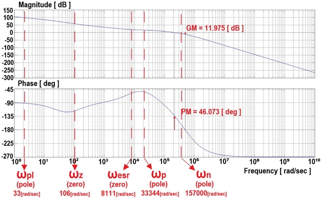
Fig. 9 is the Bode plot of the control-voltage-to-output-voltage Gvci(s) and Fig. 10 is the Bode plot of T2(s) in the current control mode.
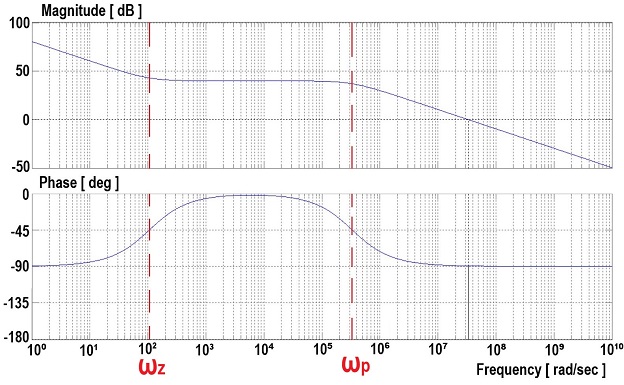
Fig. 11 is the Bode plot of the two-pole single-zero voltage compensator. Fig. 7 shows the voltage-mode control of the converter. At ωo = 876 rad/s, the phase changes rapidly from 0 to -180°, and at ωesr = 8111 rad/s, the phase increases owing to the zero. Fig. 8 shows the voltage compensator of the two poles and single zero in Fig. 11, and the zero is located at ωz = 106 rad/s while the poles are located at ωp = 33344 rad/s.
In the loop transfer function T1(s) of voltage-mode control, the gain margin (GM) is 225.58 dB and phase margin (PM) is 44.845°. In the voltage-mode control of the converter, the GM increases to 225.58 dB owing to the rapid change in the phase from 0 to -180° at ωo = 876 rad/s in T1(s), resulting in slightly degraded response characteristics.
Fig. 9 shows the current-mode control of the converter, with one pole at ωpl = 33 rad/s, one zero at ωesr = 8111 rad/s, and another pole at ωn = 157000 rad/s. Because of the single pole, the phase does not change rapidly compared to that of the voltage-mode control. Fig. 10 shows the voltage compensator of the two poles and one zero in Fig. 11, where the zero is located at ωz = 106 rad/s and pole is located at ωp = 33344 rad/s. The current-mode control of the converter has one pole at ωpl = 33 rad/s, one zero at ωz = 106 rad/s, and ωesr = 8111 rad/s in T2(s). This is characterized by one zero at ωp = 33344 rad/s and one pole at ωn = 157000 rad/s.
In the loop transfer function T2(s) of current-mode control, the GM is 11.975 dB and PM is 46.073°. In T2(s) of current-mode control, the phase change is not sharp but gradually slows down, so it is predicted that the system will operate more stably.
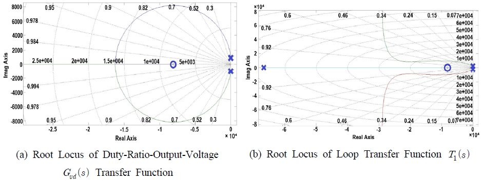
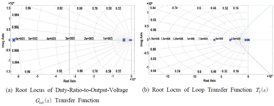
Fig. 12 shows the root trajectory plots of Gvd(s) and T1(s) in the voltage control mode, and Figure 13 shows the root trajectory plots of Gvci(s) and T2(s) in the current control mode. In the voltage control mode, the system is very slow because both Gvd(s) and root trajectory diagram of T1(s) exist in the left half of σ = 0 as the gain increases. However, in current-mode control, in terms of the root trajectory diagrams Gvci(s) of T2(s) and , the system moves to the right half of the plane as the gain increases. To improve the response characteristics of the system, the poles can be set on the left half-plane close to σ = 0, thus further improving the response characteristics.
6. Experimental Results of Flyback Converter for LED Power
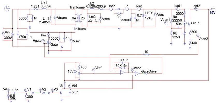
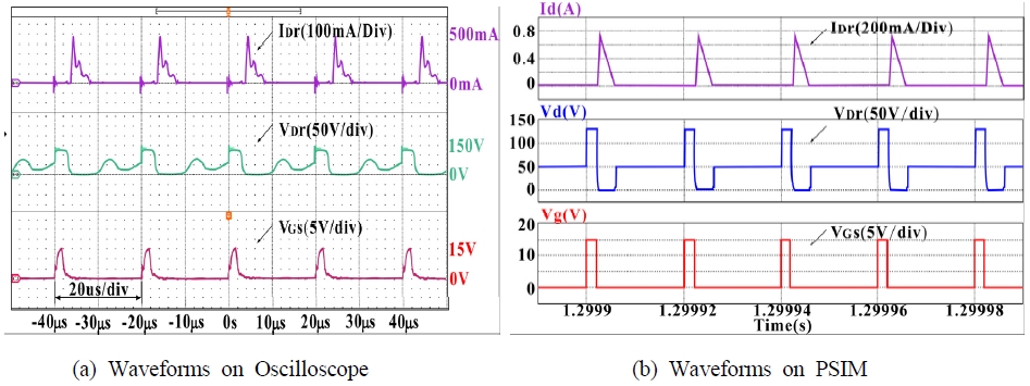
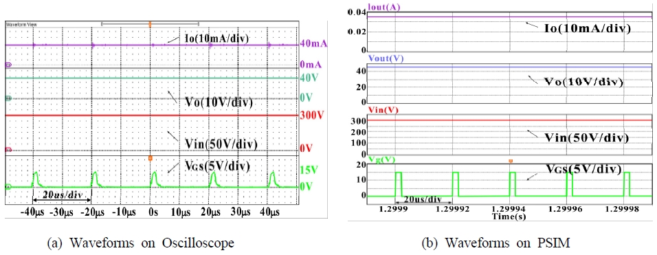
Fig. 14 shows the simulation results of the system circuit created using PSIM. Fig. 15 shows the flyback converter circuit board and system experimental setup. The system experiments were obtained from PSIM software simulation results and oscilloscope display data. Fig. 16 shows the switching current and voltage waveforms, Fig. 17 shows the transformer primary current and voltage waveforms, Fig. 18 shows the diode current and voltage waveforms, and Fig. 19 shows the input–output current and voltage waveforms. As can be seen in Figures 16~19: Comparing between the experimental waveforms and the PSIM simulation waveforms. The PSIM simulation waveform represents a very ideal waveform. However, the experimental waveform is affected by parasitic capacitors and transformer winding capacitors in the main switch (S) and diode (D).
In addition, a phenomenon in which the parasitic inductance of the circuit wiring resonates with the parasitic capacitor occurs.
Therefore, the parasitic capacitor of the main switch causes a current spike in the switch current waveform at the turn-on state of the switch.
In the voltage waveforms of the main switch and the transformer, the phenomenon of LC resonance between the parasitic capacitor and the parasitic inductor can be confirmed.
It can be seen that there is a difference in the gate signal waveform due to the charging and discharging of the gate capacitor of the main switch.
By comparing the data results, the actual detection data of the flyback converter is seen to be very similar to the PSIM simulation results.
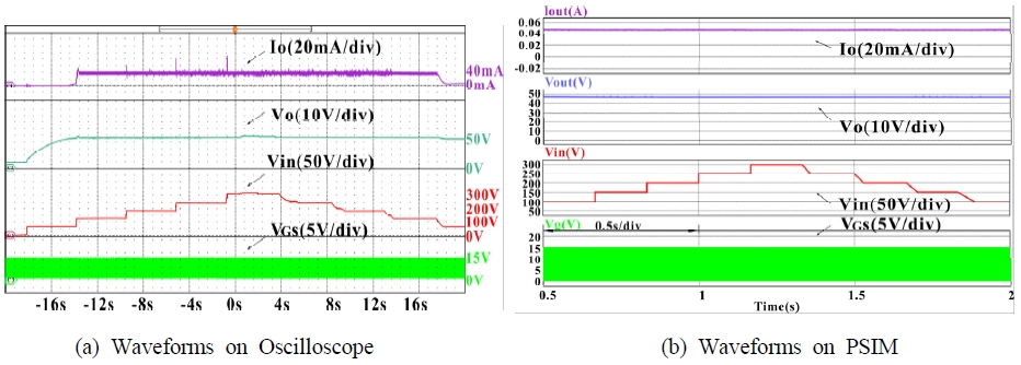
Fig. 20 shows the detection results of the output current and voltage when the input voltage is varied from 0 to 300 V. When the input voltage rises from 0 to 100 V, the output current and voltage gradually rise to the desired values and remain stable; when the input voltage drops to 100 V or below, the output current gradually decreases and output voltage decreases slightly.
Fig. 21 shows the output state results when the load resistance varies between 1,000 Ω and 500 Ω. The output current and voltage do not show any jitter or changes when the load is changed and continue to remain at the ideal value.
7. Conclusions
In this study, the design and modeling of a flyback converter and its related components for an LED power supply system are investigated and experimented. Based on the flyback converter model of the LED power system, the duty-cycle-to-output-voltage transfer function is derived for the voltage-mode control, and the control-voltage-to-output-voltage transfer function is derived for the current-mode control. The MATLAB simulation results show that in voltage-mode control, when the response frequencies 876 rad/s, the phase varies severely from 0 to -180°, which needs to be compensated by the voltage compensator in a timely manner. In current-mode control, The current mode control T2(s) with GM = 11.975 dB, PM = 46.073° is obtained and its phase change is seen to be gradually slow, and it can be determined that the system will operate stably in this mode.
▹Loop transfer function T1(s) of the voltage-mode control: GM = 225.58 dB, PM = 44.845°.
▹Loop transfer function T2(s) of the current-mode control: GM = 11.975 dB, PM = 46.073°.
Experiments on the flyback converter circuit system for an LED power supply load show the superiority of the system design. By comparing the actual experimental results with the PSIM simulation results are extremely similar, the system current feedback control and response is good and verify that the current control mode has stable pulse-width control over the duty cycle of the switching signal for pulse-width modulated output.
After theoretical study and practice, it is proved that the current control mode is the ideal mode for LED flyback switching circuits. Ignoring interference such as parasitic inductance and capacitance of power lines and components, suitable components and parameters are selected after repeated experiments, which are more conducive to realize the design function and verify the theoretical and design values.
Author contributions
L. Bai; Data curation, Formal analysis, Investigation, Validation, Visualization, Writing, Editing. J. Y. Bae; Conceptualization. Methodology. Resources. Software Simulation. Supervision.
References
- W. Steve, 2008,“Power Supply for LED Driving”, Elsevier, 149-160.
-
Z. Zhang and K. D. Ngo, 2017, “Multi‐Megahertz Quasi‐Square‐Wave Flyback Converter Using eGaN FETs”, IET Power Electronics, 10(10), 1138-1146.
[https://doi.org/10.1049/iet-pel.2016.0782]

-
V. K. Yadav, A. K. Verma and U. R. Yaragatti, 2022, “An Integrated Single-Stage Single-Switch Topology with Reduced Nonlinear Components for LED”, IEEE Journal of Emerging and Selected Topics in Industrial Electronics, 4(1), 317-326.
[https://doi.org/10.1109/JESTIE.2022.3207701]

-
H. H. Chou, 2022, “Design and Implementation of the Linear LED Driver”, IEEE Transactions on Circuits and Systems II: Express Briefs, 70(3), 1059-1063.
[https://doi.org/10.1109/TCSII.2022.3219226]

-
H. Li, S. Li, W. Xiao and S. Y. R. Hui, 2022, “A modulation method for capacitance reduction in active-clamp flyback-based AC–DC adapters”, IEEE Transactions on Power Electronics, 37(8), 9455-9467.
[https://doi.org/10.1109/TPEL.2022.3157743]

-
Q. S. Qian, S. Y. Xu, S. Y. Xu, Q. Liu, S. Ding, C. Gu and W. F. Sun, 2022, “High Precision Primary Side Regulation Constant Voltage Control Method for Primary and Secondary Resonant Active Clamp Flyback Converter”, IEEE Journal of Emerging and Selected Topics in Power Electronics, 10(6), 6985-6999.
[https://doi.org/10.1109/JESTPE.2022.3181809]

-
D. Ð. VRAČAR and P. V. PEJOVIĆ, 2022, “Active-clamp flyback converter as auxiliary power-supply of an 800 V inductive- charging system for electric vehicles,” IEEE Access, 10, 38254-38271.
[https://doi.org/10.1109/ACCESS.2022.3165059]

-
S. Xu, X. M. Zhang, C. Wang and W. F. Sun, 2016, “High Precision Constant Voltage Digital Control Scheme for Primary Side Controlled Flyback Converter”, IET Power Electronics, 9(13), 2522-2533.
[https://doi.org/10.1049/iet-pel.2015.0771]

-
D. Đ. Vračar, 2022, “Quasi-Resonant Flyback Converter as Auxiliary Power-Supply of an 800 V Inductive-Charging System for Electric Vehicles”, IEEE Access, 10, 109609-109625.
[https://doi.org/10.1109/ACCESS.2022.3214526]

-
J. H. Choi, H. M. Kwon and J. Y. Lee, 2022, “Design of a 3.3 kW/100 kHz EV Charger Based on Flyback Converter With Active Snubber”, IEEE Transactions on Vehicular Technology, 71(7), 7161-7170.
[https://doi.org/10.1109/TVT.2022.3168625]

-
X. Q. Guo, S. F. Wu, Y. R. Zhang, C. J. Dou and Y. C. Chi, 2022, “Optimal Design of High Frequency Transformer for High Power Density Flyback Converter”, IEEE Transactions on Circuits and Systems II: Express Briefs, 69(11), 4399-4403.
[https://doi.org/10.1109/TCSII.2022.3184724]

-
T. N. T. Tran, H. C. Wang and J. M. Wang, 2022, “A Dual-Mode Control Scheme to Improe Light Load Efficiency for Active-Clamp Flyback Converter. Electronics”, 11(9), 1308.
[https://doi.org/10.3390/electronics11091308]

-
T. Mohammad, D. O. Bamgboje and T. S. Hu, 2021, “Compensated Single Input Multiple Output Flyback Converter”, Energies, 14(Art. 3009), 1-23.
[https://doi.org/10.3390/en14113009]

-
N. S. Jayalakshmi, D. N. Gaonkar and A. Naik, 2017, “Design and Analysis of Dual Output Flyback Converter for Standalone PV/Battery System,” International Journal of Renewable Energy Research, 7(3), 1032-1040.
[https://doi.org/10.20508/ijrer.v7i3.5825.g7134]

-
R. B. Ridley, 1991, “A New Continuous Time Model for Current Mode Control”, IEEE Transactions on Power Electronics, 6(2), 271-280.
[https://doi.org/10.1109/63.76813]

-
F. D. Tan and R. D. Middlebrook, 1995, “A Unified Model for Current-Programmed Converters”, IEEE Transactions on Power Electronics, 10(4), 397-407.
[https://doi.org/10.1109/63.391937]

-
B. Choi, 1997, “Step Load Response of a Current Mode Controlled DC to DC Converter”, IEEE Transactions on Aerospace and Electronics Systems, 33(4), 1115-1121.
[https://doi.org/10.1109/7.624347]

-
R. W. Erickson, S. Cuk and R. D. Middlebrook, 1982, “Large Signal Modeling and Analysis of Switching Converters”, Power Electronics Specialists Conference, 240-250.
[https://doi.org/10.1109/PESC.1982.7072414]

-
R. Ridley, B. H. Cho and F. C. Lee, 1988, “Analysis and Interpretation of Loop Gains of Multiloop-Controlled Switching Regulators”, IEEE Transactions on Power Electronics, 3(4), 489-498.
[https://doi.org/10.1109/63.17971]

-
B. Choi, 2021, “Pulsewidth Modulated DC-to-DC Power Conversion: Circuits, Dynamics, Control, and DC Power Distribution Systems”, John Wiley & Sons, 198-244.
[https://doi.org/10.1002/9781119454489]

-
A. S. Raj, A. M. Siddeshwar, K. P. Guruswamy, C. M. Maheshan and S. C. Vijay, 2015, “Modelling of Flyback Converter Using State Space Averaging Technique”, 2015 IEEE International Conference on Electronics, Computing and Communication Technologies (CONECCT), 1-5.
[https://doi.org/10.1109/CONECCT.2015.7383871]

-
J. Y. Bae, 2019, “A Flyback DC/DC Converter Modeling and Controller Design for the LED-Battery System Using PV (Photovoltaic) Energy”, Journal of the Korean Institute of Illuminating and Electrical Installation Engineers, 33(8), 14-24.
[https://doi.org/10.5207/JIEIE.2019.33.8.014]

-
C. Yang, F. Xie, Y. Chen, W. Xiao and B. Zhang, 2020, “Modeling and Analysis of the Fractional-Order Flyback Converter in Continuous Conduction Mode by Caputo Fractional Calculus”, Electronics, 9(Art. 1544). (http://creativecommons.org/licenses/by/4.0/, )
[https://doi.org/10.3390/electronics9091544]

-
T. Suntio, 2006, “Average and Small-Signal Modeling of Self-oscillating Flyback Converter with Applied Switching Delay”, IEEE Transactions on Power Electronics, 21(2), 479-486.
[https://doi.org/10.1109/TPEL.2005.869760]

-
Z. Y. Zhang, H. X. He, J. J. He, H. Yu, K. Bian and W. J. Chen, 2022 “Modeling of a Flyback Converter Controlled by an IGBT for Generating a High-Frequency Pulse Voltage”, IEEE Transactions on Electron Devices, 69(6), 3262-3270.
[https://doi.org/10.1109/TED.2022.3165731]

-
S. Y. Tseng and J. H. Fan, 2022, “Zeta/Flyback Hybrid Converter for Solar Power Applications,” Sustainability, 14(5), 2924.
[https://doi.org/10.3390/su14052924]


